首页 > 代码库 > [转载]建立时间和保持时间
[转载]建立时间和保持时间
http://referencedesigner.com/tutorials/si/si_02.php
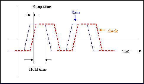
The Concept of Setup and Hold Time can be best understood with the picture shown below. 
The curve shows a clock and a data signal. The Data signal latches at the rising edge of the clock. The clock signal is in Red and Data Signal is in blue.
Set up time is the amount of time before the clock edge that the input signal needs to be stable to guarantee it is accepted properly on the clock edge. Hold time is the amount of time after the clock edge that same input signal has to be held before changing it to make sure it is sensed properly at the clock edge.
Setup and Hold times are vigourously simulated at the Chip design level to ensure that they meet the specification. As a PCB Designer our job is to make sure that we do not deteriorate them as the clock and data signals propogate along the PCB.
Let us assume that IC A is the source of a Clock and a Data Signal. The IC B is the destination of the Clock and the data signal. In its simplest form usually the clock and the data signals will have their length matched and and there will not change in the setup time when the signal leaves IC A to when it reaches B. If however, the length of the Clock Signal is is much smaller than the length of the Data signal, the setup time will get reduced at the signals reach IC B.
Whether this will cause aq failure will depend upon edge rate, clock frequency the setup time specification of the IC B. For example for a clock source of 1 MHz frequecy and slow edge rate we know pretty much sure that it will not create a setup time violation. For 100 MHz clock source we would like to do a quick calculation as to how much mismatch is allowed. For 1 GHz clock and fast edge rates we must do calculation and take special cares as dictated by the Bus technology and the setup time requirements of the destination IC.
In the next chapter we will see how to calculate the flight time of the signals as it propogates along the PCB.
[转载]建立时间和保持时间
